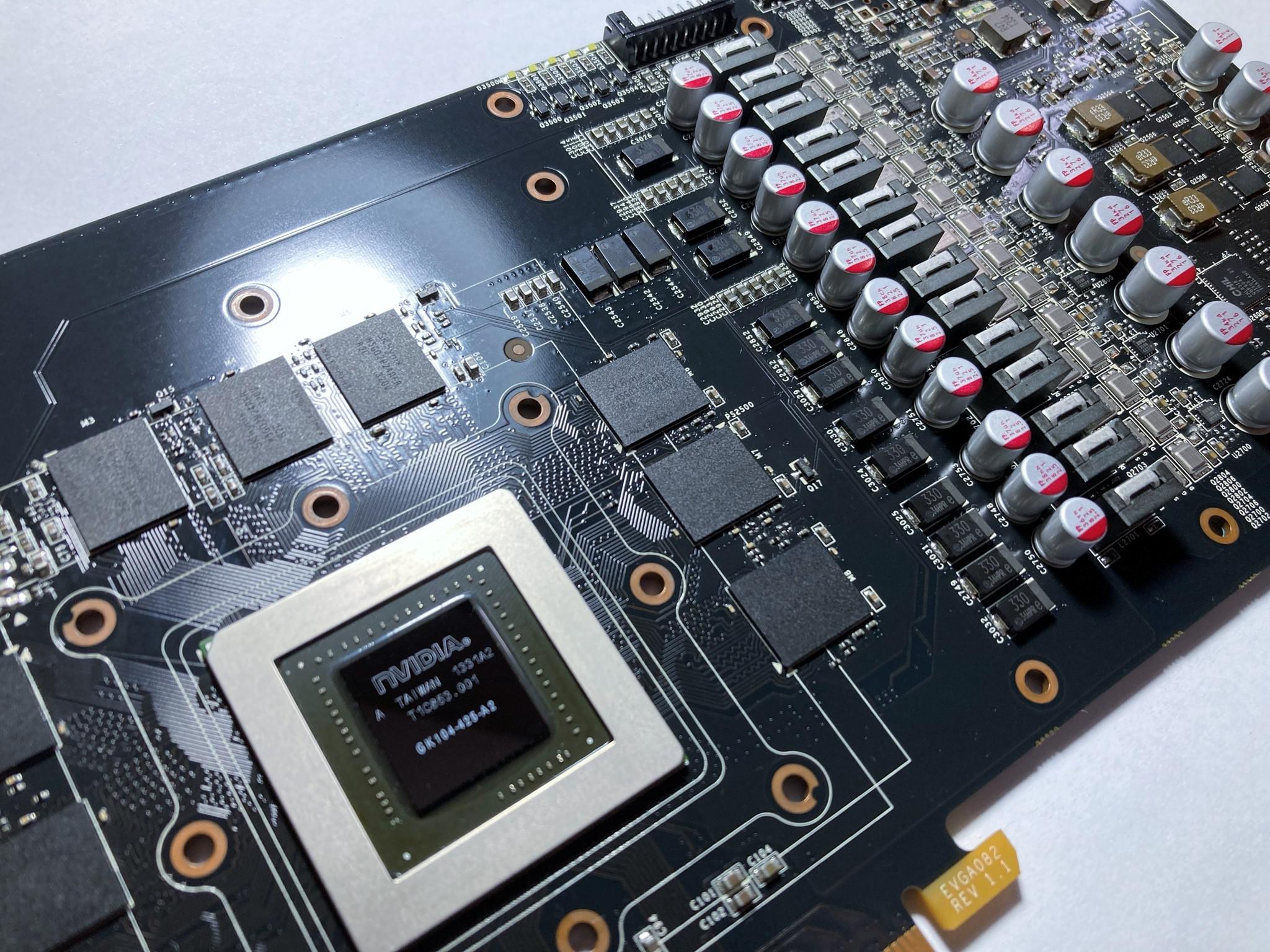
The size difference between the GPU and VRM is comical. Scariest part is the GPU can draw that much. game pcOver ClockingPC 4 Comments fliesenschieber 3 years ago It’s actually pretty insane if you think about it 3DprintRC 3 years ago 200 W through that little 17×17 mm square. UserInside 3 years ago And that’s just a Kepler GPU, which none of them got over 250W (if my memory is still correct).Now OP, imagine what a 4090 ADA102 PCB would look like in real ? Ballerfreund 3 years ago EVGA GeForce GTX 680 Classified?I guess the VRMs are the two flat rows with metal caps between the silver/red capacitor rows, so not really visible in this picture.Write A CommentYou must be logged in to post a comment.
UserInside 3 years ago And that’s just a Kepler GPU, which none of them got over 250W (if my memory is still correct).Now OP, imagine what a 4090 ADA102 PCB would look like in real ?
Ballerfreund 3 years ago EVGA GeForce GTX 680 Classified?I guess the VRMs are the two flat rows with metal caps between the silver/red capacitor rows, so not really visible in this picture.

4 Comments
It’s actually pretty insane if you think about it
200 W through that little 17×17 mm square.
And that’s just a Kepler GPU, which none of them got over 250W (if my memory is still correct).
Now OP, imagine what a 4090 ADA102 PCB would look like in real ?
EVGA GeForce GTX 680 Classified?
I guess the VRMs are the two flat rows with metal caps between the silver/red capacitor rows, so not really visible in this picture.